Instrument Overview:
The xenon plasma source achieves higher beam currents than conventional gallium liquid metal source FIB. This results in an order-of-magnitude improvement in milling rates, and thus allows for high-speed / large-area cross-sectioning and large volume 3D tomography applications.
The xenon plasma source also allows for gallium-free sample preparation using inert xenon ions, which facilitates contamination-free preparation of samples which may be susceptible to alteration or contamination by conventional gallium FIB processing.
A range of electron detectors allow for high resolution imaging, and simultaneous acquisition of topographic and compositional contrast. A dedicated SEM-STEM detector allows ultra-high resolution imaging of electron transparent samples in Bright Field, Dark Field and High Angle Annular Dark Field imaging modes.
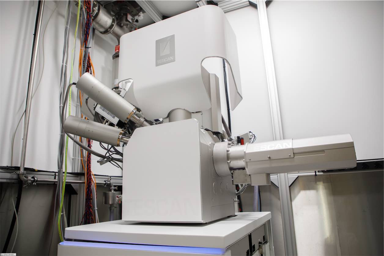
PFIB microscope integrated in radiation-shielded research room
Complementary analytics in the form of EBSD and EDX detectors allow for the acquisition of compositional (elemental composition) and crystallographic (phase distribution, crystallographic orientation, grain size and morphology) information respectively. Used in conjunction with FIB-SEM tomography, these analytics allow for in-situ, static, 3D EBSD and EDX analysis of large 3D volumes representative of bulk material.
This instrument is also equipped with Pt and C gas injection systems (GIS) for deposition of protective layers, a rotatable micro-manipulator needle for lift-out or manipulation of test pieces, and a rocking stage which can be used in conjunction with TESCAN’s TRUE X-sectioning method to reduce curtaining and ‘waterfall’ effects, thus improving the quality of surface finish.
Applications:
- High-speed / large-area cross-sectioning
- Large volume 3D tomography
- Surface or cross-sectional EBSD (phase distribution, crystallographic orientation, grain size and morphology) and EDX (elemental composition) analysis
- 3D EBSD and EDX analysis
- Gallium-free sample preparation (e.g. TEM lamellae or APT) needles
- Large microcantilever preparation
- Ultra-high-resolution Imaging (including SEM-STEM)
- Transmission Kikuchi Diffraction analysis (ultra-high-resolution phase distribution, crystallographic orientation, grain size and morphology)
Reconstruction of a 3D volume of EUROFER 97 low-activation steel showing grain orientation determined from 3D EBSD data (45 x 55 x 30 µm volume)
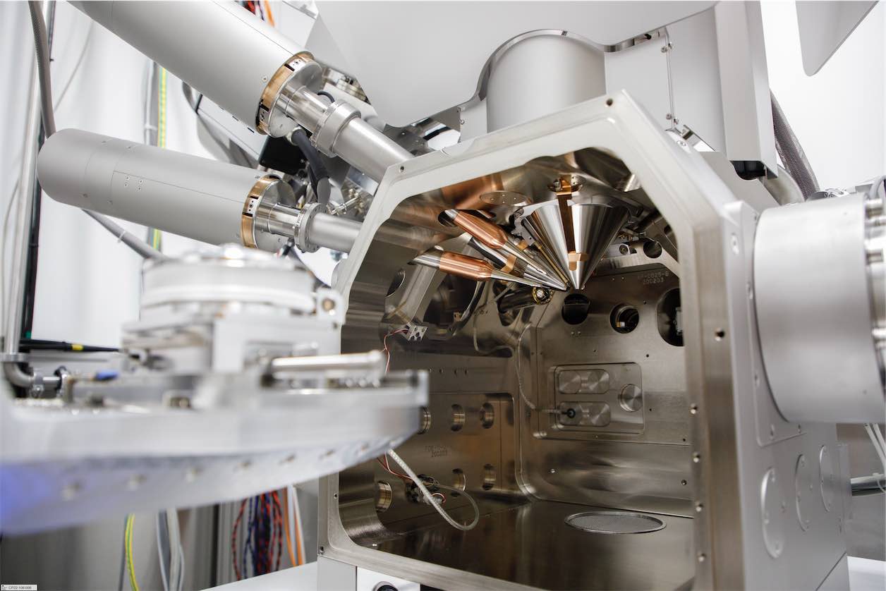
PFIB sample chamber
Technical Specification:
- Schottky thermal field-emission electron gun for high-resolution imaging
- Xenon ion source for milling
- Pt and C deposition capabilities
- Large voltage and probe current range:
- Electron-beam: 500 V – 30 Kv, 2 pA – 400 nA
0.9 nm resolution (15 kV)
(*0.8 nm in STEM mode, 30 kV) - Ion-beam: 3 kV – 30 kV, 1 pA – 3 µA
<12 nm resolution (30 kV)
- Electron-beam: 500 V – 30 Kv, 2 pA – 400 nA
- 5-axes compucentric stage with unique multi-tilt (rocking ± 9°) functionality, -60 – +90° tilt range, infinite rotation
- Chamber and in-lens SE & BSE detectors, dedicated retractable BSE detector
- SEM-STEM detector capable of BF, DF & HADF imaging
- Complementary Analytics:
- EBSD: Oxford Instruments Symmetry S2 (>4500 EBSP / s, 0.05° angular resolution)
- EDX: Oxford Instruments Ultimax 170 (large sensor area)