Instrument Overview:
The instrument is equipped with a full range of detectors for multi-scale characterisation of samples.
- Secondary electron detector (SE) sensitive to sample’s topography changes.
- Backscattered-electron detector (BSE) which provides imaging that carries information on the sample’s composition.
- Energy-dispersive x-ray (EDX) allowing chemical characterisation of materials.
- electron backscatter diffraction detector (EBSD) for microstructural-crystallographic characterisation of samples.
Applications:
- High resolution microscopy
- Grain size analysis
- Post corrosion studies
- Porosity measurements
- Chemical composition (±1 at%)
Technical Specification:
- High brightness Field Emission Gun (Schottky emitter) for high-resolution/ high current/ low-noise imaging (up to 70nA of beam current)
- Resolution up to 1.2nm at 30kV
- Oxford Instruments X-Max 80 EDX detector (can detect elemental composition including Be)
- Oxford Instruments Symmetry 2 EBSD detector (up to 4500 patterns per second acquisition)
- Sample holders for Transmission Kikuchi Diffraction (TKD)
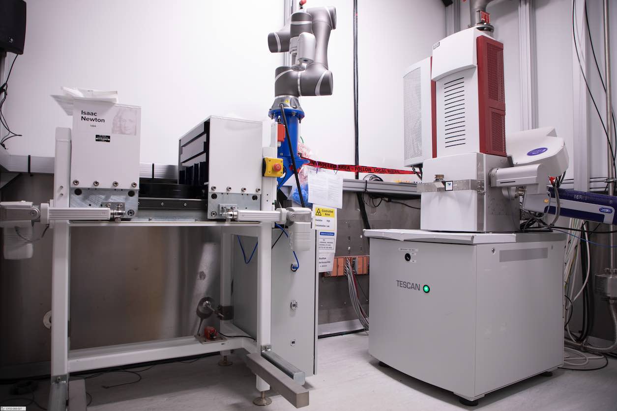
The Tescan scanning electron microscope in its research room
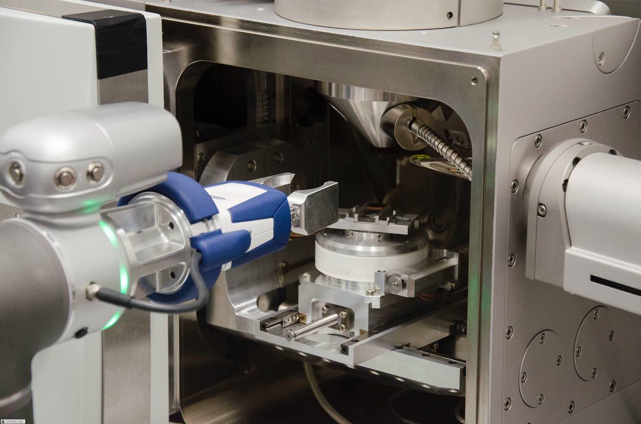
The TESCAN scanning electron microscope being remotely loaded
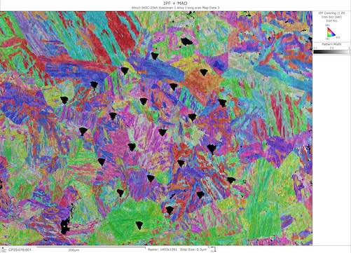
EBSD image of reactor pressure vessel steel with an array of indents for correlating mechanical properties with crystal orientation
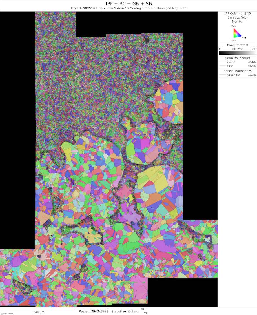
EBSD image of G91/316 steel bond