Instrument Overview
Raman spectroscopy uses a laser to probe a sample to investigate the roto-vibrational states with in it, these can inform on chemical properties, chemical identification, bonding states, stress, etc. The laser light is absorbed by the sample, which is then re-emitted with a slightly different wavelength, this is known as the Raman shift. The confocal microscope system is able to track the height of the sample and interpret it to measure surface topography. This then allows 3D images to be constructed. Raman and topographical information can be acquired simultaneously.
The system has additional capabilities in the form of Atomic Force Microscopy, AFM, and Scanning Near Field Optical Microscopy, SNOM, options as well as an environmental stage for controlled atmosphere or vacuum and temperatures up to 1500°C.
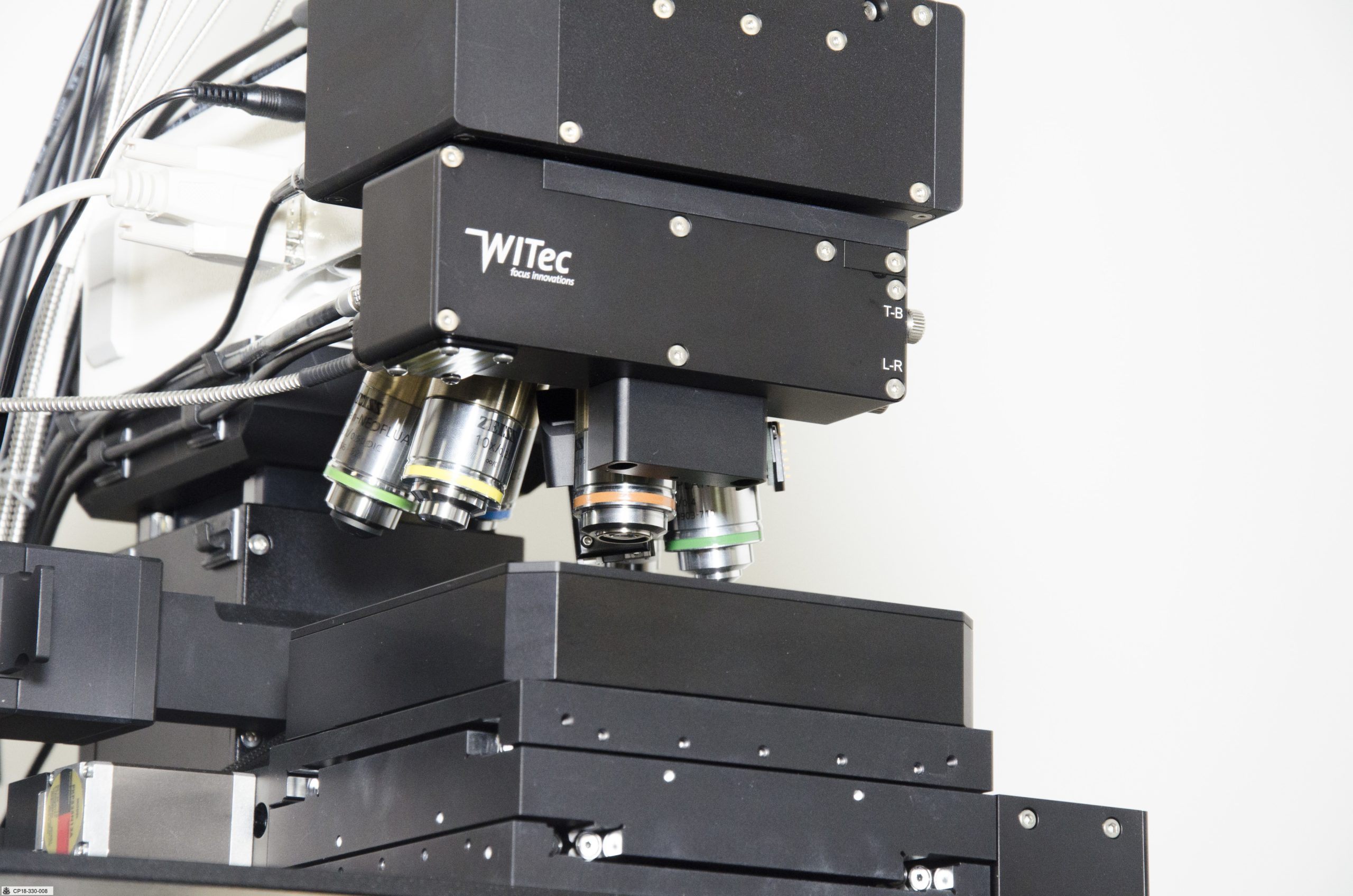
WITec Alpha 300 ARS Confocal Raman Microscope.
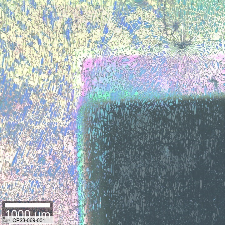
Optical Image Stitch of Grade 91 steel with alumina coating. Irradiated with 35 MeV Au6+ ions at 550°C for 64 hours, the dark area was masked off from the ion beam.
Applications
- Material / Chemical identification and structure.
- Material phase and polymorphy.
- Determination of crystallinity.
- Determination of stress and strain.
- Profilometry of sample surface
- In-situ testing via an environmental stage; heat treatments, annealing, oxidation, etc
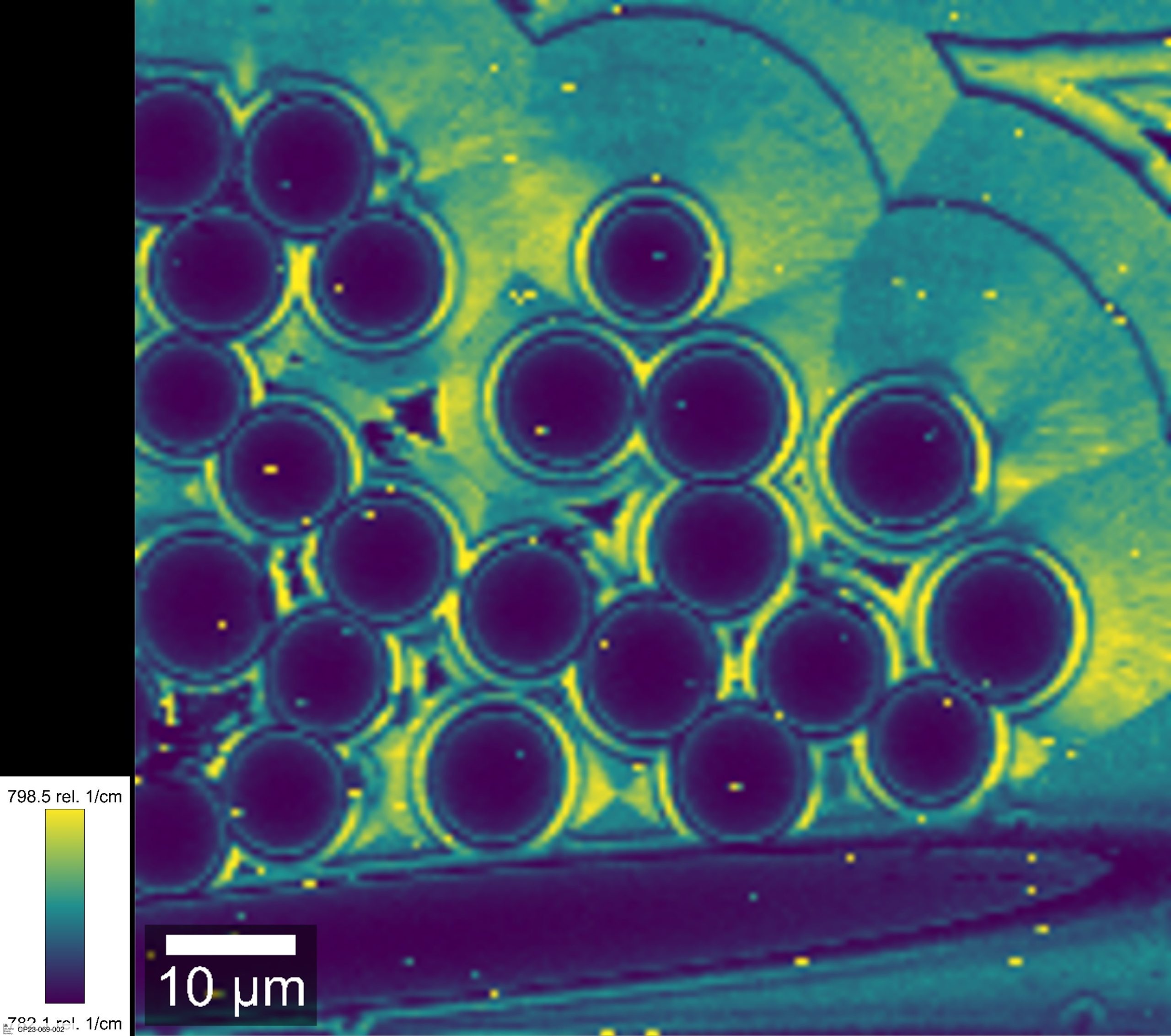
Raman map of SiCf/SiC showing the shift in peak position, highlighting areas of stress.
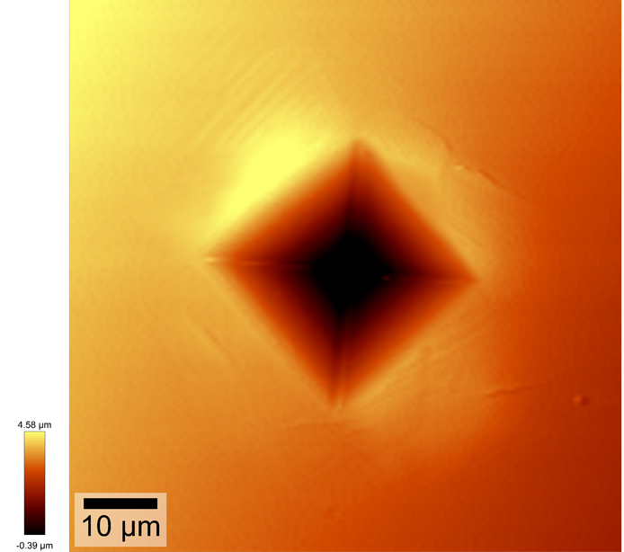
True Surface ™ scan of a nanoindentation in copper, showing pile up and slip bands.
Technical Specification:
- Confocal bright field microscopy in reflection mode.
- Magnification lens carousel with 6x lenses including long working distance lens.
- Image and video acquisition.
- Large area optical mapping, up to 25x25mm.
- True Surface™ profilometry over large areas.
- Fluorescence and Raman spectroscopy.
- X-Y mapping
- Depth profiling and scanning
- Excitation wavelengths: 457nm, 532nm, 633nm.
- Gratings: 600 and 800 l/mm.
- Spectral resolution: 0.72cm-1.
- Detectors, CCD and, EMCCD for ultra-rapid acquisition.
- Automated positioning and acquisition available.
- AFM option:
- Profilometry over small areas.
- Contact and non-contact modes
- SNOM option:
- Allows for optical resolution of Raman spectra down to 90nm.
- Linkam TS1500 Environmental Stage option
- Maximum temperature of 1500°C
- Up to 200°C/min ramp rate.
- Choice of purge atmospheres, or vacuum.
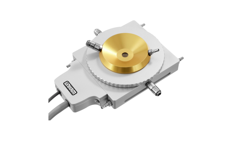
Linkam TS1500 Environmental Stage. This replaces the piezo stage under the microscope to enable in situ testing.